ENVIRONMENT AND ENERGY
Simulation of Magnetic Fingerprints of Interface Defects in Silicon Solar Cells
Principal Investigator:
Prof. Dr. Wolf Gero Schmidt
Affiliation:
Theoretical Materials Physics Group, Paderborn University (Germany)
Local Project ID:
AdFerro1
HPC Platform used:
Hermit and Hornet of HLRS
Date published:
Leveraging the high-performance computing capabilities of the HLRS supercomputing infrastructure, scientists of the Theoretical Materials Physics Group of the Paderborn University managed to trace interface defects in amorphous/crystalline silicon heterojunction solar cells. Visualizing the processes with atomic resolution they were able to characterize the processes that compromise the solar cells' efficiency. The findings will help to optimize the solar cells further and to decrease production costs.
While in principal silicon-based solar cells could turn up to 30 percent of the power contained in sunlight to electricity, in reality different loss mechanisms ensure that even under ideal lab conditions the maximum efficiency does not exceed 25 %. In particular recombination at defects and grain boundaries, where electrons and holes meet and recombine, is detrimental in solar cells. Advanced heterojunction cells are designed to address this problem: On top of the crystalline Silicon (c-Si) surface a thin layer of disordered amorphous hydrogenated silicon (a-Si:H) is deposited. This thin film saturates many of the interface defects and conducts charge carriers out of the cell. Heterojunction solar cells have already high efficiencies of up to 24 % – even in industrial scale. However, scientists had until now only a rough understanding of the processes at the remaining interface defects.
Using a electrically detected magnetic resonance (EDMR) spectra, physicists from the Helmholtz-Zentrum Berlin für Materialien und Energie (HZB) have managed to actually trace the interface defects in amorphous/crystalline silicon heterojunction solar cells: Thereby the spin of the defect-localized electrons is used as a probe that provides a magnetic fingerprint in the photo current of the solar cell under a magnetic field and microwave radiation.
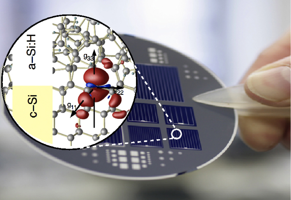
In order to interprete the spectral signatures the Theoretical Materials Physics group in Paderborn performed extensive computer simulations on the structure, electronic properties and magnetic response of the c-Si/a-Si:H interface. Thereby the realistic modeling of the amorphous material – that lacks longe-range order and needs to be modeled with very large supercells – was one of the technical challenges, which could only be met by using massively parallel high-performance computing resources. The defects' exact locations could be determined by means of a detailed comparison between the EDMR data with density functional theory (DFT) g tensor calculations of interface states. There are basically two distinct families of electronic defect states: a-Si:H conduction band tail states and two different paramagnetic dangling bond states directly at the [111]-oriented buried c-Si surface, cf.

Fig. 1: Calculated magnetization density at an c-Si/a-Si:H interface defect.
Copyright: Theoretical Materials Physics Group, Paderborn UniversityFor the first time ever it has thus become possible to detecting and characterizing processes with atomic resolution that compromise the solar cells' efficiency. The cells were manufactured and measured at the HZB; the numerical methods were developed at Paderborn University within a program sponsored by the Deutsche Forschungsgemeinschaft (DFG priority program 1601). These findings will now help to optimize the solarcells further and to decrease production costs.
Reference:
BM George, J Behrends, A Schnegg, TF Schulze, M Fehr, L Korte, B Rech, K Lips, M Rohrmüller, E Rauls, WG Schmidt, U Gerstmann “Atomic Structure of Interface States in Silicon Heterojunction Solar Cells“,
Phys. Rev. Lett. 110, 136803 (2013), doi: 10.1103/PhysRevLett.110.136803
Scientific contact:
Prof. Dr. Wolf Gero Schmidt
Lehrstuhl für Theoretische Materialphysik, Universität Paderborn
D-33095 Paderborn (Germany)
e-mail: W.G.Schmidt @ upb.de
http://physik.uni-paderborn.de/ag-schmidt/