
MATERIALS SCIENCE AND CHEMISTRY
Ab Initio Simulation of Materials for Si-Compatible Microelectronics
Principal Investigator:
Dr. Jarek Dabrowski
Affiliation:
IHP – Leibniz-Institut für innovative Mikroelektronik, Frankfurt (Oder), Germany
Local Project ID:
IHPms21
HPC Platform used:
JUWELS CPU at JSC
Date published:
Abstract
The IHPms21 project combined advanced computer simulations with experimental techniques to develop new materials for future microelectronics that are compatible with silicon technology. Using ab initio density functional calculations, the project helped interpret experimental results and guide further research. The team achieved three key outcomes: first, they explained why germanium surfaces behave differently depending on their orientation during graphene growth; second, they uncovered how multilayer hexagonal boron nitride (hBN) can grow from an inert gas, despite its chemical inactivity; and third, they analyzed photoemission spectra to reveal the presence of ultrathin β-Ga2O3 films on the surface of ZnGa2O4 crystals.

Figure1. Atomic structures. Carbon (C) is black, hydrogen (H) is blue, nitrogen (N) is green, and boron (B) is brown. (a) Molecules: CH4 (methane), C6H6 (benzene), and B3N3H6 (borazine). (b-c) 2D materials: Graphene and hBN. (d) 3D crystal: Germanium (Ge). Two cleavage planes, (001) and (110), are indicated by blue lines. The plane of the picture is Ge(110) as well.
Overview
The IHPms21 project, which ran from May 2021 to April 2024 on the JUWELS supercomputer, combined atomic-scale simulations with experimental work. The goal was to develop new materials for microelectronics that could improve performance without requiring expensive changes to existing silicon chip technology. Simulations can support such innovations by providing insights into complex physical processes and guiding experimental efforts [1]. Researchers at IHP are investigating how two-dimensional (2D) materials, like graphene and hexagonal boron nitride (hBN), could be used in devices such as high-frequency transistors, optical communication systems, and sensors.
One of the biggest challenges in this research is finding ways to produce high-quality, chemically clean, and easy-to-handle films of these materials. For practical use, these films need to be compatible with standard chip manufacturing processes and, ideally, grown directly on the chips, rather than transferred from another surface.
The project focused on two key materials: graphene, a highly conductive 2D material (Fig. 1b), and hBN, a 2D insulator with a honeycomb structure similar to graphene but made of alternating boron and nitrogen atoms (Fig. 1b). The films were grown on silicon wafers, commonly used in microelectronics, which were coated with a thin layer of germanium (Fig. 1c), a semiconductor that is compatible with silicon technology. These experiments were conducted under conditions similar to those used in actual chip production, but also in more flexible, lab-based environments.
By modeling complex physical processes at the atomic level, the simulations provided valuable insights that guided the experimental work. The project used a technique called density functional theory (DFT), which is based on quantum mechanics. Although DFT is computationally intensive, it helps scientists understand how atoms interact with each other and is essential for designing new materials at the smallest scales.
In these simulations, the atomic structures of materials were optimized by calculating quantum-chemical forces between atoms. Most of the calculations were performed using the Quantum Espresso software package [2], which models electron interactions in a way that balances accuracy with efficiency. The method focuses on the electrons involved in chemical reactions (the valence electrons) and treats core electrons using simplified "pseudopotentials" to speed up the calculations. In some cases, more detailed calculations were performed using the NWChem software [3], which provided additional insights into the electronic behavior of the materials.
IHPms21 was closely linked to the EU FLAG-ERA JTC project “2DHetero: hBN/Graphene 2D Heterostructures: from scalable growth to integration” [4], which aimed to develop new methods for growing graphene (Fig. 1b) and hexagonal boron nitride (hBN, Fig. 1c) films on germanium surfaces (Fig. 1d). These films were produced at IHP using chemical vapor deposition (CVD), a technique in which hot substrates are exposed to gases that carry the elements needed to form the films. CVD is favored in established chip manufacturing processes. Methane (CH4, Fig. 1a) was used for graphene growth, while borazine (B3N3H6, Fig. 1a) was used for hBN, with molecular hydrogen (H2) playing a key role in both processes. The simulations investigated how 2D flakes of graphene and hBN nucleate, grow, and merge on the catalytic germanium surface and how the growth of hBN continues even after the catalyst is deactivated by the hBN coating. They also helped explain the growth rates observed in the experiments.
In addition to graphene and hBN, the project also studied the surface properties of ZnGa2O4 (ZGO) surfaces. ZGO a transparent oxide material that could improve high-power electronics and deep-ultraviolet (UV) light devices. Recent advances in the production of ZGO crystals with high structural quality [5] made it possible to examine the surface preparation techniques needed for their application in electronic devices.

Figure2. (a-d) Factors influencing the behavior of Ge(110) and Ge(001) during graphene growth by CVD from CH4. Blue squares in panels a and b indicate Ge atoms evaporating as volatile GeH4, full circles represent carbon atoms, red circles in panel d illustrate the additional C incorporated due to enlargement of the surface area by faceting. Schematic side view; adapted from [10]. (e-f) Initiation of a (107) facet ridge, where (e) graphene edge bonds to flat Ge(001), followed by (f) adsorption of Ge vacancies at the bonded boundary, and (g) expansion of the bonded boundary onto the new (107) facet. Surface Ge atoms are well known to form pairs (dimers) arranged in rows, see the red circle pairs in panel a. Ge atoms are shown in red (terrace A), blue (terrace B), and sepia (subsurface), while carbon atoms are black. Atoms forming C-Ge bonds are enlarged. Edge carbon atoms not bonded to Ge are hydrogen-saturated. Domain B terraces (blue) can be viewed as accumulations of Ge vacancies on domain A terraces (red), and vice versa. Ge(107) is composed of alternating domain A and B terraces (panel g). Realistic top and schematic side views; adapted from [11] and [10].
Morphologie evolution of Ge surfaces during growth of graphene
Graphene, a single layer of carbon atoms arranged in hexagons (Fig. 1b), is an exciting material for advanced electronics. Researchers at IHP are studying how it grows on silicon wafers covered with thin germanium (Ge) layers (Ge/Si), both in controlled lab settings [6,7,8,9] and under conditions suitable for mass production [10,11]. Both silicon and germanium are semiconductors with a diamond-like atomic structure (Fig. 1d), but graphene can be grown only on germanium and not on silicon or diamond. Among various possible orientations of the Ge surface (Fig. 1d), Ge(110) tends to give the best results for graphene growth, though Ge(001) is more relevant for industrial applications. Understanding the intrinsic differences in the responses of these two surface orientations during the growth process is crucial, as it clarifies that the variations in graphene quality on Ge(001) are rooted in these fundamental characteristics, guiding future research and development strategies.
At the atomic scale, the responses of Ge(110) and Ge(001) to graphene growth by chemical vapor deposition (CVD) are markedly different: Ge(110) becomes smoother: Ge(110) becomes smoother (Fig. 2a), while Ge(001) roughens, as it forms nanoscale facets—tiny regions where the surface shifts from (001) to (107) orientation (Fig. 2b-g). This roughening is problematic because it creates uneven graphene with hills and valleys that can impact its performance in electronic devices.
The evolution of the Ge surfaces is driven by several factors (Fig. 2a-d), such as the formation of surface vacancies caused by hydrogen etching, the diffusion of vacancies to step edges, terrace consumption, and the formation of facets that stabilize steps. For Ge(001), the process is especially complicated by the formation of (107) facets, which align with the growing front of graphene flakes and expand together with them (Fig. 2e-g).
During CVD, methane (CH4) is used to supply carbon atoms for graphene growth. When CH4 interacts with the Ge surface, it breaks down into carbon and hydrogen atoms. The surface becomes covered with a mix of carbon-hydrogen fragments, which then migrate across the surface and condense into graphene at edges graphene flakes (Fig. 2e). Alternatively, C atoms may dissolve in the germanium crystal, while hydrogen may evaporate, either as alone as H2 or together with germanium as GeH4. The behavior of these fragments depends on factors such as substrate temperature, the concentrations of CH4 and H2 in the gas, and the presence of nearby graphene flakes.
On Ge(001), larger graphene flakes tend to prevail at surface steps. These steps match the optimal distance between the graphene and the substrate, reducing strain in the graphene. The crystallographic alignment between Ge(001) and graphene is optimal when graphene edges bond at specific angles, which are set by the intersection of Ge(001) and Ge(10n) planes. In particular, the Ge(107) plane (n = 7) provides a low-energy surface for bonding, allowing graphene flakes to expand along it (Fig. 2f-g). These facets grow, because the bonded edge attracts the Ge vacancies formed as a result of Ge evaporation in the form of GeH4. Graphene can spread onto new terraces, leading to more efficient growth and coverage of the surface (Fig. 2c-d).
In contrast, Ge(110) does not form new terraces during graphene growth. Its more complex surface structure prevents the concerted formation of new graphene together with new nanoscale facets. The vacancies created by GeH4 desorption cause the surface to smooth out: they remove step edges instead of creating new ones (Fig. 2a). The contrasting responses of Ge(001) and Ge(110) to CVD growth of graphene are fundamentally linked to their intrinsic surface properties, highlighting that the variations in graphene quality are less influenced by adjustable growth parameters and more by the inherent characteristics of the materials.
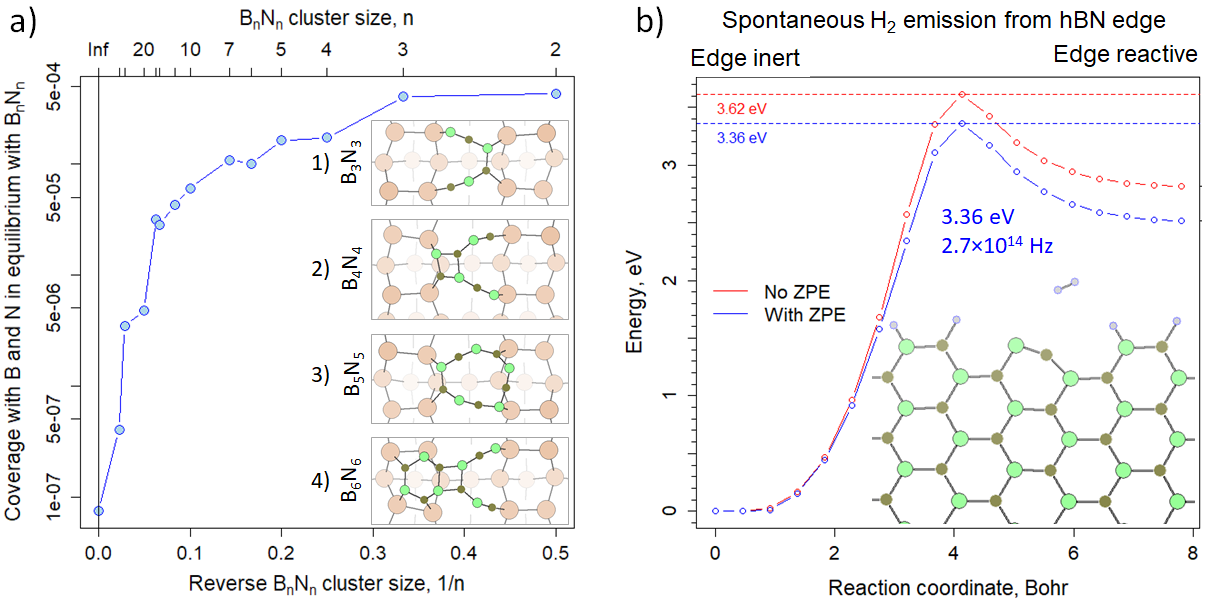
Figure 3. (a) Equilibrium coverage of Ge(001) with B and N atoms at 900°C in the presence of stoichiometric BnNn. B is brown, N is green, H is blue, Ge is sepia. The smallest BN clusters prefer localizations between Ge(001) surface dimer rows and do not maximize the number of closed B3N3 rings. (b) Self-activation of the armchair edge in multilayer hBN through spontaneous H2 emission from an edge BN dimer, with and without Zero Point Energy (ZPE) correction. ZPE is a quantum-mechanical effect, which changes energy relations by imposing vibrations. Inclusion of this effect, often neglected in larger systems for computational costs, was in this particular case important.
Growth of mono- and multilayer hBN films on Ge(001) substrates
Hexagonal boron nitride (hBN) is a 2D wide band-gap insulator with a hexagonal lattice (Fig. 1c), structurally similar to graphene (Fig. 1b), which is a 2D conductor. Films of hBN were grown on Ge(001) via chemical vapor deposition (CVD) using borazine (B3N3H6, Fig. 1a) at IHP and atomic B and N at IEMN [4]. Experimental data was gathered using a range of characterization techniques, including spectroscopic (Raman and photoemission), microscopic (STM, TEM, SEM, AFM), and electrical methods (e.g., fabrication of simple electronic devices).
The IHPms21 project supported this work by investigating the physical mechanisms and chemical pathways governing the growth process, including surface reactions, seed nucleation and expansion, defect generation and annihilation, and the morphological response of the substrate surface. From a theoretical perspective, the problem required the treatment of a large number of structures and transitions, with the project database now containing nearly 30,000 structures. These range in size from isolated atoms and molecules to periodic clusters of over 1,000 atoms. Access to the JUWELS cluster was crucial for handling these computational demands.
Monolayer flakes of hBN grow on germanium in a similar manner to graphene. The inert B3N3H6 gas is chemisorbed and partially decomposed on the Ge substrate, with its fragments (or atomic B and N, depending on the precursor) forming clusters that collect material from their surroundings. Figure3a demonstrates this for the case of atomic B and N as precursors. As the hBN flake grows, the equilibrium concentration of B and N in the surrounding area decreases, reflecting the increasing stability of the flake. Similar to small carbon clusters, stable BiNi clusters with up to eleven atoms (Fig. 3a, insets 1-3) lack six-membered rings at all, while the B6N6 cluster (Fig. 3a, inset 4, twelve atoms) has only one six-membered ring and its remaining B and N atoms are arranged in a complex way resembling that in the B4N4 cluster (Fig. 3a, inset 2). This is an edge effect, observed even in large flakes. Such short, long, or open rings at hBN edges may play a significant role in forming defects at the boundaries between coalescing flakes. They may be responsible for imperfect coalescence even when the flakes share the same crystallographic orientation and would be otherwise expected to merge seamlessly into a large, perfect 2D flake. These boundary defects include screw dislocations, which in turn can drive continuous multilayer growth without the need for new nucleation sites. Screw dislocations convert a multilayer film into a structure resembling a multi-storey park, where all levels are interconnected by ramps and may be viewed as a single plane interwoven with itself.
Notably, hBN growth indeed does not stop when the Ge surface is fully covered. Instead, growth continues at a constant rate, whether borazine or atomic precursors are used. This contrasts with graphene, where multilayer growth under similar CVD conditions and temperatures requires precursor activation (breaking the molecules, at least by removing a hydrogen atom from such precursors as methane or benzene, cf. Fig. 1a). In the case of hBN, we found that activation occurs at the edges of hBN flakes (Fig. 3b). Unlike graphene, where hydrogen termination stalls growth unless the temperatures are impracticably high, efficient emission of H2 from hBN edges maintains a virtually hydrogen-free growth front when the temperature exceeds unproblematic 800°C. While the sticking probability of B3N3H6 to a hydrogenated BN dimer is essentially zero (due to the high energy barrier for H2 desorption), the same molecule attaches to a hydrogen-free BN dimer with near-100% probability. This is because the energy barrier for attachment is virtually eliminated, and pre-orientation of the molecule through physisorption on the hBN surface increases the probability that the impinging molecule collides with the edge with its own edge and not with its face (Fig. 1a): physisorbed borazine sticks to hBN surface with its face, not with its edge, so that it already constitutes a tiny, mobile (and volatile) new “layer”.
At a constant temperature, the degree of edge activation decreases with increasing H2 partial pressure. However, the armchair edge remains largely hydrogen-free even at H2 pressures two to three orders of magnitude higher than the total chamber pressure during hBN deposition. While this holds at thermodynamic equilibrium, the computed rate of spontaneous H2 emission from the edge (3·1016 Hz, Fig. 3b) suggests that equilibrium is reached only after a time slightly longer than the average interval between two consecutive collisions of borazine with the same edge dimer, given the experimental borazine pressure (10-6 mbar). The computed growth rates, based on simulated step flow velocity and step distance estimated from TEM (transmission electron microscopy) images, align with the experimentally observed rates across different temperatures and pressures.
Alternative activation mechanisms were also considered, such as H out-diffusion along screw dislocations, catalytic activation of B3N3H6 or H2 on hot chamber elements, or activation at orientational grain boundaries in hBN. Of these, activation on hot elements ranks second in plausibility but appears incompatible with the low-temperature and low-pressure growth of hBN observed experimentally. Therefore, spontaneous H2 emission (Fig. 3b) remains the most likely explanation for the observed growth behavior.

Figure 4. UV He II photoemission spectrum from ZGO covered by ultrathin β-Ga2O3 layer, as simulated from DFT data using (a) site-independent and (b) site-dependent Hubbard U. Note the spurious shoulder on the high-energy (left-hand) side of the O 2p peak in panel a, and the difference in the energy axis range. Blue points represent the experimental photoemission spectra from the same processed sample. The two simulations assumed slightly different mean elastic free paths for the photoelectrons, but this only affected the bulk contribution, with no significant influence on the appearance of the shoulder. Adapted from Ref. 14.
Photoemission from ZGO surfaces
During the first year of the project, a study carried out in collaboration with the Leibniz-Institut für Kristallzüchtung (IKZ) and the Institute of Physics at Humboldt University, Berlin and focused on the effects of surface preparation on the chemical composition of ZnGa2O4(001) surfaces was completed [14,15]. Ab initio calculations were performed for numerous atomic surface and near-surface structures with varying stoichiometry and surface periodicity, and the corresponding photoemission spectra were computed. These computed spectra, along with measured UV photoemission and experimental XPS data for core states (Fig. 4), provided the basis for identifying the surface chemistry. Without theoretical support, this identification would have been difficult.
The calculations explored a variety of numerical approximations, testing the effects of pseudopotentials and the exchange-correlation energy (GGA, Hubbard U, HSE hybrid) on the photoemission spectra. It was found that the simulated photoemission was significantly influenced by the dependence of the Hubbard U parameter on the chemical environment of the atoms. This factor is often overlooked but causes substantial shifts in the energies of oxygen states in the topmost two layers. Consequently, spectra simulated for the correct structure may exhibit artificial features, such as the shoulder seen in Fig. 4a. These artifacts can complicate analysis and may even lead to premature rejection of the structure under investigation.
Approach
Atomic structures were optimized by relaxing the atoms based on quantum-chemical forces. In most cases, these forces were calculated using the density functional theory (DFT) via the open-source package Quantum Espresso [2]. DFT computes the spatial distribution of electron density, which is then used to derive such quantities as energies and forces. It approximates electrons as separate particles, each one described by its own quantum-mechanical wave function, and adds a so-called exchange and correlation functional to enhance accuracy. In most calculations the popular PBE functional was used [16], while reliability of the key results was tested with the B3LYP hybrid functional [17]. Hybrid functionals augment the exchange energy by a contribution calculated in a more strict way, albeit the price is a significant increase in computational effort. Dispersive (van der Waals) interactions were treated using the RVV10 scheme [18].
Quantum Espresso represents electron wave functions with plane waves (periodic oscillations, reminiscent of sine and cosine functions), an efficient method for periodic systems. Only valence electrons, which are directly involved in chemical reactions, were explicitly included, while core electrons were treated within the pseudopotential approach, where they are considered frozen in their atomic states. To evaluate the impact of these approximations, isolated molecular systems were also calculated using an all-electron basis set via the open-source code NWChem [3], employing many-particle theory at the MP2 level [19]. The DFT contribution to the correlation energy was calculated using the B2PLYP double-hybrid functional [20].
Summary and conclusions
IHPms21 combined ab-initio density functional calculations with experimental work to develop material solutions for Si-compatible microelectronics. The simulations aided in the interpretation of measurements and provided valuable insights that contributed to the planning process. The project identified why the morphology of Ge surfaces with two orientations, (001) and (110), evolves oppositely during graphene growth from methane. It also uncovered the mechanism enabling the chemically inactive multilayer hexagonal boron nitride to grow from inert borazine. Through disclosing the physical background of the processes that influence the preparation of these modern materials, the new knowledge acquired by the project may assist the development of technology needed to realize the application of 2D films (graphene, hBN, and their stacks) in such devices as field-effect-transistors [21], novel vertical transistors [22,23], photodetectors [24], sensors [25], or qubits [26]. The usefulness of DFT in laboratory work is further illustrated by the DFT-based analysis of photoemission spectra from ZnGa2O4 crystals, which revealed ultrathin β-Ga2O3 films on their surfaces. This material has potential to improve high-power electronics and deep-UV optoelectronic devices [27]. The calculations simulate complex quantum-mechanical interactions in thousands of structures often containing many hundreds of atoms, necessitating the usage of supercomputing clusters like the JUWELS cluster. This research lays the groundwork for future studies aimed at advancing the integration of 2D materials in next-generation electronic devices.
Acknowledgments
The calculations were performed with a grant of computer time provided by the John von Neumann Institute for Computing on the JUWELS cluster at the Jülich Supercomputing Centre (JCS) in the compute project IHPms21. J.D., F.A., M.F., and M. L. gratefully acknowledge funding from the EU FLAG-ERA project 2DHetero [4].
Bibliography
[1] J. Dabrowski and E. Weber (eds), Predictive Simulation of Semiconductor Processing: status and challenges (Springer-Verlag, Berlin, Heidelberg, 2004).https://link.springer.com/book/10.1007/978-3-662-09432-7
[2] P. Giannozzi, S. Baroni, N. Bonini, et al., QUANTUM ESPRESSO: a modular and open-source software project for quantum simulations of materials, J. Phys. Cond. Mat. 21, 395502 (2009) https://arxiv.org/abs/0906.2569; What Can Quantum Espresso Do? http://www.quantum-espresso.org/whatcanqedo.php
[3] E. Apra, E. J. Bylaska, W. A. de Jong, et al., NWChem:Past, present, and future, J. Chem. Phys. 152, 184102 (2020) https://doi.org/10.1063/5.0004997; NWChem: High-Performance Computational Chemistry, https://www.nwchem-sw.org
[4] 2DHetero: hBN/Graphene 2D Heterostructures: from scalable growth to integration, https://www.flagera.eu/wp-content/uploads/2020/06/FLAG-ERA_JTC2019_GRA-BR_2DHetero.pdf.
[5] Z. Galazka, S. Ganschow, R. Schewski, et al., APL Materials7, 022512 (2019). https://www.researchgate.net/publication/329668563_Ultra-wide_bandgap_conductive_high_mobility_and_high_quality_melt-grown_bulk_ZnGa_2_O_4_single_crystals
[6] G. Lippert, J. Dabrowski, T. Schroeder, et al., Graphene grown on Ge(001) from atomic source, Carbon 75, 104 (2014). https://arxiv.org/abs/1312.5425
[7] J. Dabrowski, G. Lippert, and G. Lupina, Initial state of graphene growth on Ge(001) surfaces, ECS Transactions 69, 345 (2015). https://iopscience.iop.org/article/10.1149/06905.0345ecst
[8] J. Dabrowski, G. Lippert, J. Avila, et al., Understanding the growth mechanism of graphene on Ge/Si(001) surfaces. Scientific Rep. 6, 31639 (2016). https://www.nature.com/articles/srep31639
[9] A. Becker, Ch. Wenger, and J. Dabrowski, Influence of temperature on growth of graphene on germanium. J. Appl. Phys. 128, 045310 (2020). https://doi.org/10.1063/5.0003234
[10] F. Akhtar, J. Dabrowski, R. Lukose, C. Wenger, and M. Lukosius, Chemical Vapor Deposition Growth of Graphene on 200 mm Ge(110)/Si Wafers and Ab Initio Analysis of Differences in Growth Mechanisms on Ge(110) and Ge(001), ACS Appl. Mater. Interfaces 15, 36966 (2023). https://pubs.acs.org/doi/10.1021/acsami.3c05860
[11] F. Akhtar, Graphene synthesis under Si-CMOS compatible conditions, PhD thesis, BTU Cottbus, 25 Apr 2022. https://opus4.kobv.de/opus4-btu/files/5927/Akhtar_Fatima.pdf
[12] M. Franck, J. Dabrowski, M. A. Schubert, C. Wenger and M. Lukosius, Towards the Growth of Hexagonal Boron Nitride on Ge(001)/Si, Nanomaterials12, p. 3260, 2022. https://www.mdpi.com/2079-4991/12/19/3260
[13] M. Franck, J. Dabrowski, M. A. Schubert, D. Vignaud, M. Achehboune, J.-F. Colomer, L. Henrard, C. Wenger, and M. Lukosius, Investigating Impacts of Local Pressure and Temperature on CVD Growth of Hexagonal Boron Nitride on Ge(001)/Si, accepted for publication in Advanced Materials Interfaces (2024).
[14] F. Reichmann, J. Dabrowski, A. P. Becker, et al., Experimental and Theoretical Investigation of the Surface Electronic Structure of ZnGa2O4(100) Single-Crystals. Phys. Stat. Sol. B 2021, 210045 (2021). https://d-nb.info/124833308X/34
[15] F. Reichmann, Germanium, Tin and (Zinc) Gallium Oxide for Advanced Micro- and Optoelectronics: Insights into the Surface Electronic Structure with Photoemission Techniques, PhD thesis, BTU Cottbus, 2 Dec 2022. https://opus4.kobv.de/opus4-btu/files/6208/Reichmann_Felix.pdf
[16] J. P. Perdew, K. Burke, and M. Ernzerhof, Generalized gradient approximation made simple. Phys Rev Lett. 77, 3865 (1996). https://dft.uci.edu/pubs/PBE97.pdf
[17] P. J. Stephens and F. J. Devlin and C. F. Chabalowski and M. J. Frisch, Ab Initio Calculation of Vibrational Absorption and Circular Dichroism Spectra Using Density Functional Force Fields, J. Phys. Chem. 98, 11623 (1994) and references therein. https://apps.dtic.mil/sti/pdfs/ADA291297.pdf
[18] R. Sabatini, T. Gorni, and S. de Gironcoli, Nonlocal van der Waals density functional made simple and efficient, Phys. Rev. B 87, 041108(R) (2013). https://www.researchgate.net/publication/258015017_Nonlocal_van_der_Waals_density_functional_made_simple_and_efficient
[19] M. Head-Gordon, J. A. Pople, and M. J. Frisch, MP2 energy evaluation by direct methods. Chemical Physics Letters. 153, 503 (1988). https://doi.org/10.1016/0009-2614(88)85250-3
[20] S. Grimme, Semiempirical hybrid density functional with perturbative second-order correlation. J. Chem. Phys. 124, 34108 (2006). https://doi.org/10.1063/1.2148954
[21] S. Fukamachi, P. Solís-Fernández, K. Kawahara, et al. Large-area synthesis and transfer of multilayer hexagonal boron nitride for enhanced graphene device arrays. Nature Electronics 6, 126–136 (2023). https://doi.org/10.1038/s41928-022-00911-x
[22] W. Mehr, J. Dabrowski, J. C. Scheytt, G. Lippert, Ya-Hong Xie, and M. C. Lemme, Vertical Graphene Base Transistor, IEEE Electron. Dev. Lett 33, 691 (2012). https://doi.org/10.1109/LED.2012.2189193
[23] C. Strobel, C. A. Chavarin, M. Knaut, et al., High Gain Graphene Based Hot Electron Transistor with Record High Saturated Output Current Density, Adv. Electron. Mat. 10, 2300624 (2024). https://doi.org/10.1002/aelm.202300624
[24] Haiyan Jiang, Bo Li, Yuning We, et al., High-performance gold/graphene/germanium photodetector based on a graphene-on-germanium wafer, Nanotechnology 33, 345204 (2022). https://iopscience.iop.org/article/10.1088/1361-6528/ac6ff0
[25] Chung Won Lee, Tae Hoon Eom, Sung Hwan Cho and Ho Won Jang, Chemical Sensors Based on Graphene and 2D Graphene Analogs, Adv. Sensor Research 2, 2200057 (2023). https://doi.org/10.1002/adsr.202200057
[26] L. Banszerus, K. Hecker, S. Möller. et al. Spin relaxation in a single-electron graphene quantum dot, Nat Commun13, 3637 (2022). https://doi.org/10.1038/s41467-022-31231-5
[27] M. Higashiwaki, K. Sasaki, H. Murakami, et. al., Recent progress in Ga2O3 power devices, Semicond. Sci. Technol. 31, 034001 (2016). https://iopscience.iop.org/article/10.1088/0268-1242/31/3/034001