
MATERIALS SCIENCE AND CHEMISTRY
Dynamical Processes in Semiconductor Nanostructures
Principal Investigator:
Gabriel Bester
Affiliation:
University of Hamburg and the Hamburg Centre for Ultrafast Imaging (Germany)
Local Project ID:
TDPSN
HPC Platform used:
Hazel Hen of HLRS
Date published:
Prof. Gabriel Bester (University of Hamburg and the Hamburg Centre for Ultrafast Imaging (CUI)) and his group use ab-initio density functional theory (DFT) to unravel the effects of lattice vibrations on the electronic and optical properties of semiconductor nanostructures and how they can influence carrier dynamics in the femtoseconds to tens of picosecond time range. The scientific interest resides not only in the understanding of fundamental physics (“how does matter behave at the nanometer scale?”) but also in a reliable assessment of the importance of carrier relaxation, dephasing and temperature effects, which are relevant for semiconductor nanodevices, specifically for the design and control of nanomaterials in the fields of optoelectronics, spintronics, photovoltaic, biolabeling, and the next generation of displays.
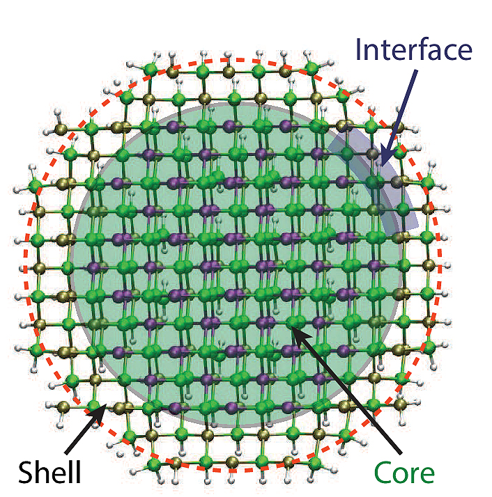
Figure 1: Atomistic models of InAs-InP core-shell nanocluster with diameter of 3 nm.
Copyright: CUI, Universität HamburgThe task is computationally most challenging. On the one hand, the chemistry is complicated due to, e.g., surface effects, which requires an expensive quantum mechanical ab-initio treatment. On the other hand, the structures, although small in size, are large in the number of atoms and number of electrons that need to be considered. In this project, the scientists pushed the boundary in terms of system size and completed calculations of semiconductor nanoclusters with diameters ranging from 2 to 3 nm (see Figure 1 for an InAs-InP core-shell nanocluster with diameter of 3 nm), which can be prepared in the laboratory and used in real applications.
The calculations within this project were performed with the CPMD code (Car–Parrinello molecular dynamics) using a combination of MPI (Message Passing Interface) and OpenMP (Open Multi-Processing) parallelism on the GCS supercomputer Hazel Hen of the HLRS. The researchers obtained near-linear scaling up to one thousand cores for the problems at hand which is excellent for the high level of complexity of the code and the extensive use of FFTs (fast Fourier transform algorithms).
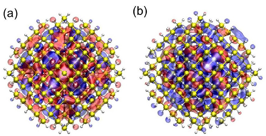
Figure 2: Electronic wave functions of (a) HOMO and (b) LUMO states for a silicon nanocluster with a diameter of 2.4 nm.
Copyright: CUI, Universität Hamburg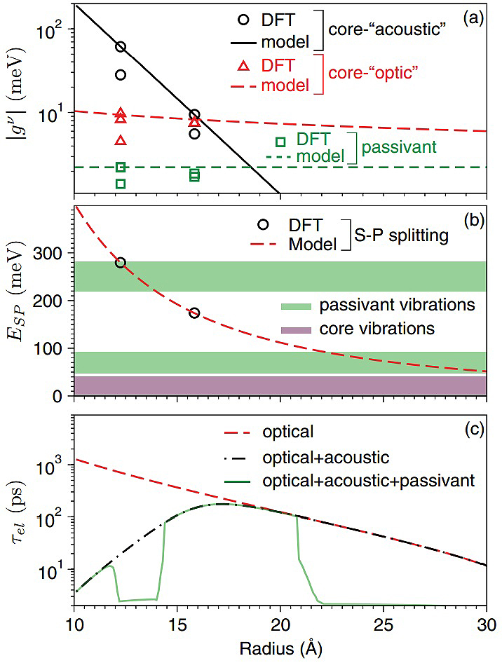
Figure 3: (a) Electron-phonon coupling strength, (b) electronic energy level spacing, and (c) carrier lifetime of InAs nanoclusters as a function of nanocluster size.
Copyright: CUI, Universität HamburgThe electronic wave functions of the highest occupied molecular orbital (HOMO) and the lowest unoccupied molecular orbital (LUMO) states of semiconductor nanoclusters, which are used to calculate the magnitude of the electron-phonon (e-ph) coupling [1, 2], are plotted in Figure 2 (a) and (b), respectively. With the calculated e-ph coupling, a size dependent carrier relaxation time of semiconductor nanoclusters induced by lattice vibrations is obtained (see Figure 3 for e-ph coupling, electronic energy level spacing, and carrier lifetime as a function of size for an InAs nanocluster [2].)
This project contributed to a fundamental understanding of the effects of size confinement—which represents the reduced dimensionality and the existence of large surface effects—on the lattice vibrations. The results achieved in this project help to establish a physical picture of ultrafast electronic processes in colloidal semiconductor nanostructures, which benefits further developments and applications of colloidal semiconductor optoelectronic devices.
References:
[1] P. Han and G. Bester, "First-principle calculation of the electron-phonon interaction in semiconductor nanoclusters", Phys. Rev. B 85, 235422 (2012).
[2] P. Han and G. Bester, "Carrier relaxation in colloidal nanocrystals: Bridging large electronic energy gaps by low-energy vibrations", Phys. Rev. B 91, 085305 (2015).
Scientific Contact:
Prof. Gabriel Bester
University of Hamburg and The Hamburg Centre for Ultrafast Imaging,
Grindelallee, 117 D-20146 Hamburg (Germany)
email:gabriel.bester [at] uni-hamburg.de
HLRS Project ID: TDPSN
June 2016