
MATERIALS SCIENCE AND CHEMISTRY
Shear-induced Phase Transitions of Silicon and Diamond
Principal Investigator:
Michael Moseler
Affiliation:
Fraunhofer IWM, Freiburg, and University of Freiburg
Local Project ID:
chfr09
HPC Platform used:
JUWELS and JURECA of JSC
Date published:
Shear stress can cause plastic deformation in crystalline materials. In soft materials such as metals this can occur through the motion of dislocations. In contrast, deformation of covalent materials such as silicon and diamond can cause the formation of thin, amorphous layers at the sliding interface. The amorphization of silicon, for example, is responsible for the nanoscale wear of silicon tips in atomic force microscopes and affects the surface quality of silicon wafers. The amorphization of diamond plays a central role in polishing of jewelry and industrial diamonds.
The elementary processes that govern friction and wear usually occur on small length scales which makes scientific studies very challenging. In experiments it is usually not possible to directly observe the processes at the sliding interface. This is often referred to as the “buried interface” problem. Therefore, research on these processes relies on simulations. In the chfr09 project presented here, simulations on atomic length scales were performed on GCS supercomputers to study the behavior of silicon and diamond under combined shear and compression. As shown in Fig. 1, the simulations show the formation of an amorphous layer with fluid-like properties. In case of silicon, the amorphous material has a lower density than the crystal. As a result, the formation of the amorphous layer is favored by pressure applied to the system from the outside. Increasing the pressure between the surfaces leads to faster formation of the amorphous layer. In case of diamond, however, the amorphous layer has a lower density than the crystal. Therefore, an increased pressure slows down amorphization.
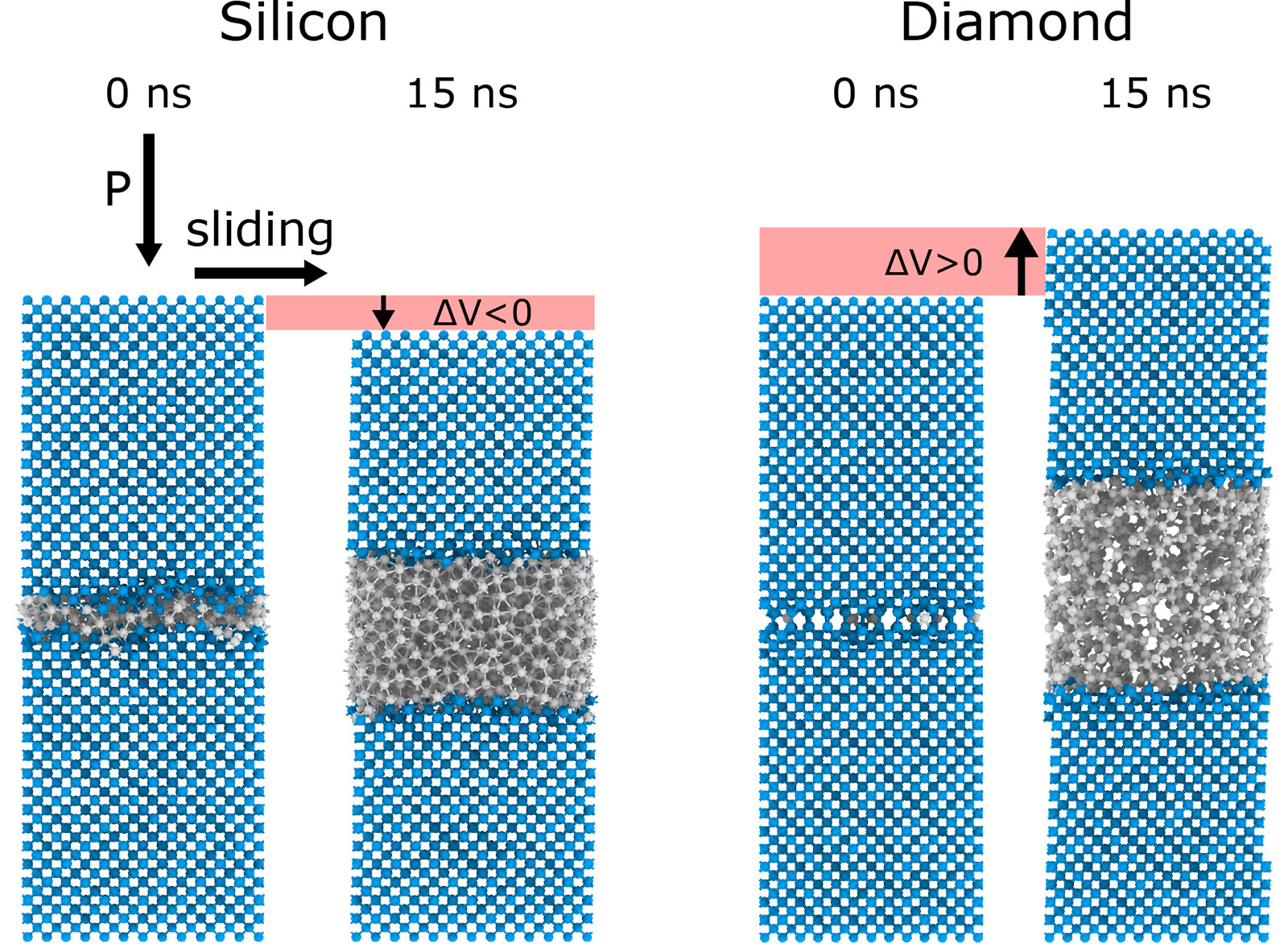
Fig.1: For both, diamond and silicon, the formation of an amorphous phase, shown here in gray, can be observed under combined compressive and shear stress. While the system contracts in the silicon case in the course of this phase transformation (ΔV<0 ), the system expands (ΔV>0) in the diamond case. As a consequence, pressure P favors silicon amorphization and suppresses diamond amorphization. © Fraunhofer IWM, Freiburg
For silicon, shear-induced recrystallization counteracts amorphization resulting in a constant thickness of the amorphous zone of only a few atomic layers for low pressures. The elastic response of silicon crystals to shear is anisotropic and therefore the pairing of differently oriented crystals can lead to the migration of the amorphous zone. As shown in Fig. 2 this results in the “triboepitaxial” growth of one crystal at the expense of the other.
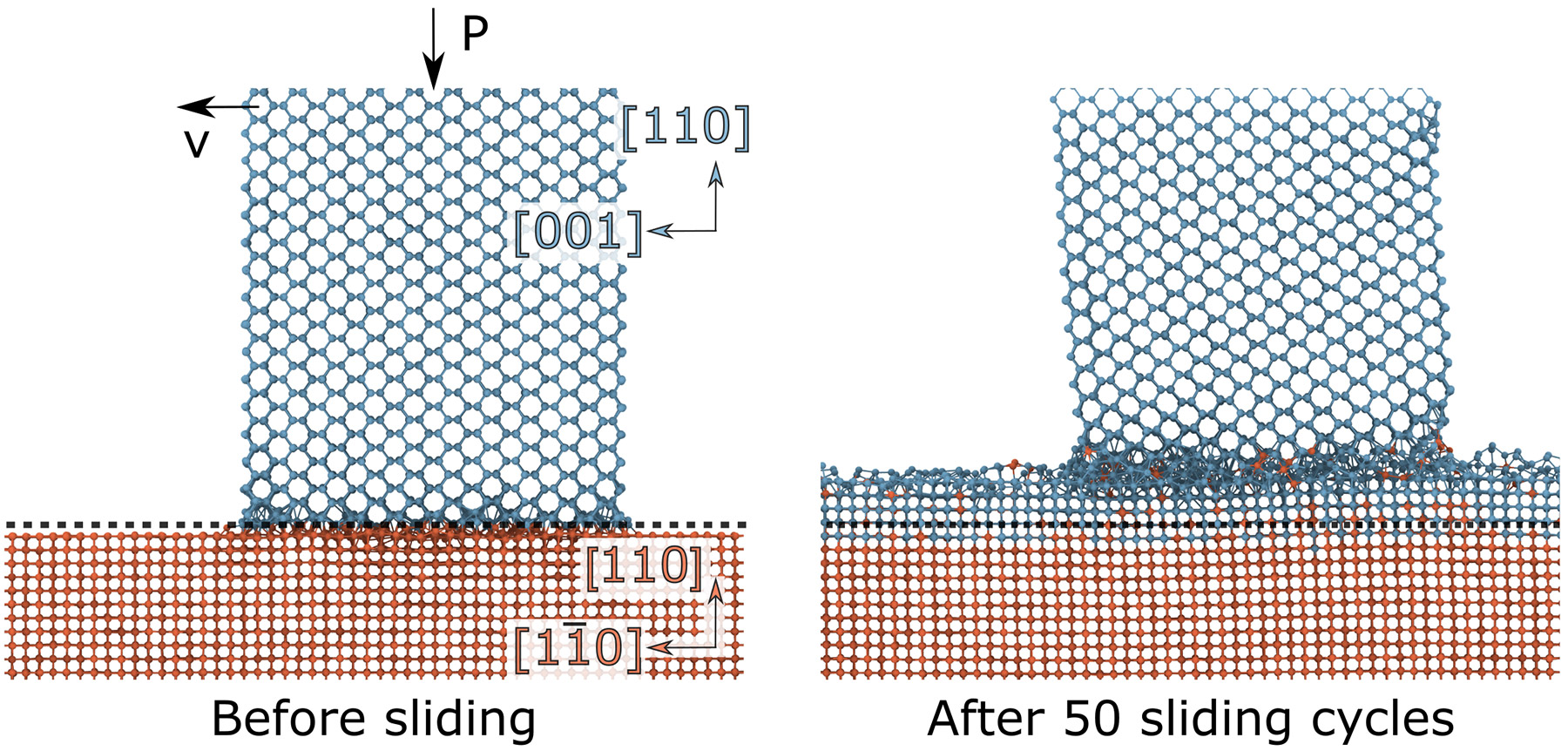
Fig.2: Sliding of two differently oriented silicon crystals can result in the growth of one crystal at the expense of the other. Atoms that are initially part of the upper and lower crystal are shown in blue and red, respectively. This concept, which we name “Triboepitaxy”, is simply controlled by the elastic response of the two crystals to shear deformation. © Fraunhofer IWM, Freiburg
Our results are in particular for silicon unexpected and have important consequences for technical applications. For example, the detailed understanding of the shear-induced phase transitions may help to improve the surface quality of silicon wafers in semiconductor manufacturing. Moreover, the “triboepitaxy” concept could be used for the direct deposition of crystalline silicon nanostructures or for the selective microstructural modification of a surface.
References
The scientific details of this project were published in the project's interim reports, as well as in the journals Physical Review Materials and Physical Review Letters:
Gianpietro Moras, Andreas Klemenz, Thomas Reichenbach, Adrien Gola, Hiroshi Uetsuka, Michael Moseler, Lars Pastewka, Shear melting of silicon and diamond and the disappearance of the polyamorphic transition under shear, Physical Review Materials 2, 083601 (2018)
Thomas Reichenbach, Gianpietro Moras, Lars Pastewka, Michael Moseler, Solid-Phase Silicon Homoepitaxy via Shear-Induced Amorphization and Recrystallization, Physical Review Letters, in press (2021).
Research Team
Dr. Gianpietro Moras1, Dr. Andreas Klemenz1, Thomas Reichenbach1, Prof. Dr. Lars Pastewka1,2, Prof. Dr. Michael Moseler1,3 (PI)
1Fraunhofer IWM, MicroTribology Center μTC, Wöhlerstraße 11, 79108 Freiburg, Germany
2Department of Microsystems Engineering, University of Freiburg, Georges-Köhler-Allee 103, 79110 Freiburg, Germany
3Institute of Physics, University of Freiburg, Hermann-Herder-Straße 3, 79104 Freiburg, Germany
Scientific Contact
Prof. Dr. Michael Moseler
Fraunhofer Institute for Mechanics of Materials (IWM), MicroTribology Center μTC
Wöhlerstr. 11, D-79108 Freiburg (Germany)
and
Department of Microsystems Engineering
University of Freiburg
Georges-Köhler-Allee 103, D-79110 Freiburg (Germany)
e-mail: michael.moseler [@] iwm.fraunhofer.de
Local project ID: chfr09
August 2021