
MATERIALS SCIENCE AND CHEMISTRY
Strain Knob to Adjust Electronic Properties of 2D Materials
Principal Investigator:
Dr. Thomas Brumme
Affiliation:
Technische Universität Dresden, Germany
Local Project ID:
inhomostrain2d
HPC Platform used:
JUWELS Booster, GPU and CPU at JSC
Date published:
Abstract
2D materials are one of the important material classes with potential to address problems with conventional semiconducting materials. They possess inherently a thin structure which can be used to manufacture even smaller electronic devices. Even if we know many different 2D materials, the ultimate use of them requires comprehensive knowledge about them and how one can expand their properties. Strain is a versatile tool to adjust 2D materials properties. It can be applied to many 2D materials intentionally, or it can be simply introduced during their synthesis. Understanding the influence of strain in this class provides important information for its employment in novel devices such as spin straintronics.
Project
One way to categorize materials is based on the way and strength their atoms are connected to each other. One of the fascinating group of materials is the Van derWaals materials in which the layers similar to a lasagna are placed layer by layer over each other. The layers are interacting only with weak forces, however the atoms in each plane are strongly chemically bonded. When the layers are separated, either using physical or chemical methods, they demonstrate novel properties due to quantum effects which become dominant in smaller sizes. There are a myriad of 2D Van der Waals materials such that material databases now exist that collect the properties of these materials.1 One of the material classes of 2D materials which the bulk version of it has already been known for several decades are transition metal dichalcogenides (TMDC) in which a transition metal such as Molybdenum, Mo, or Tungsten, W, bonds with a chalcogen such as sulfur, S, or selenium, Se atoms, to form a layered material. When a layer (i.e. a sandwich of metal atom between chalcogen atoms) of these materials is isolated, the optoelectronic properties of the material changes. For example, the monolayer of them begins to absorb light differently. It is of technological importance to have various materials with distinct properties, but it can also be interesting to adjust properties of one material by means of external fields. Several external stimuli, such as strain fields, can be used to continuously and reversibly change the materials properties. However, among them strain can provide a continuous and reversible tuning. The strain can be applied to 2D material employing the mismatches between the 2D material and its substrate, either due to a thermal expansion, a lattice size or even a strength mismatch. It has already been shown that in-plane (i.e. uni- or biaxial) strain can strongly influence the electrical properties of 2D materials; for example, by changing their band gaps, that is the difference between the filled and empty states in the electronic structure of the material. One can understand for example how the material can interact by a beam of light from the size of its band gap. 2D material are also susceptible to deformations in the out-of-plane direction due to their small bending moduli, resulting in wrinkles, bubbles and steps. These structures insert a complex strain on the system and thus change the material properties. Even though various experimental studies addressed this important issue, relatively few theoretical works investigated them thoroughly.
Obtaining theoretical insight into the electronic structures requires atomistic calculations. The size of these computational models of a wrinkled system increases drastically, particularly after breaking symmetries in the non-uniformly strained systems; therefore, many researches had to resort to many assumptions to perform calculations of these systems. Nowadays, the computational resources such as the resources that were provided by GCS for this project are an enormous help for scientists to perform accurate studies with fewer simplifying assumptions. Density functional theory calculations considering important physical effect such as spin orbit coupling had rarely been performed for those structures in the literature before the current investigation. Nevertheless, we had to limit ourselves to ground state (i.e. electronic structure) properties due to the huge size of the system. With the advancement in computational method for calculating optical properties such as lowscaling quasi particle methods like low-scaling G0W0,2,3 the investigation of these systems should be expanded to optical properties in the future.
In this project (i.e. inhomostrain2D), we performed calculations at the chair of theoretical chemistry of TU Dresden to capture the influence of strain on several 2D materials.
One important part of this project was to address the influence of the wrinkled structures in monolayer tungsten diselenide, WSe2. Additionally, to understand how simplifying assumption can affect the electronic structure, the feasibility of nanotubes as a model for wrinkled systems was examined. Even if the nanotube strain profile is not the same as the wrinkle, it still has an important feature that makes it more similar than a simple in plane strain. The atoms on each side of the metal atom experience different strain type, either tensile or compressive. The structures are then computationally relaxed to have almost no internal residual forces. As expected, the relaxed nanotubes maintained their initial profile. In contrast, the strain field in the wrinkle redistributes, resulting in peaks and valleys having the maximum strain, and inflection points with a minimum strain. Moreover, we show that curvature in addition to prior knowledge about electronic states can link the electronic structure of the wrinkle and nanotube. An important relativistic effect, spin orbit coupling (SOC), is also included in our calculations. This effect is negligible in light elements and becomes significant in heavy elements such as transition metals. Moreover, we show that SOC must be included in the electronic structure to capture the small but important characteristics of the electronic structure. Due to symmetry breaking and SOC in the structures, a splitting in electronic structure in momentum direction occurs. This splitting is similar to Rashba splitting, which occurs in uniform electron gas under an electric field. Rashba splitting also occurs in transition metal dichalcogenides with two type of chalcogens (i.e. Janus TMDCs). The Rashba-like splitting in wrinkled monolyaer of WSe2 is one order of magnitude larger than the splitting in Janus-type TMDCs and almost equals the Rashba splitting in elemental surfaces such as Au(111)4 and Ir(111).5 Interestingly, the Rashba coefficient that shows the strength of splitting in nanotubes and wrinkles is almost the same for the wrinkle and nanotube having equal curvature. This type of splitting with its sensitiveness to strain can be employed in novel spin straintronics. Moreover, strain localized the states in monolayer wrinkle WSe2, leading to transfer of the bound state of electron and hole quasi-particles (i.e. exciton) to high strain region which is referred to as exciton funneling. Although this phenomenon is well characterized in experiments, our results clarify the origin of the phenomena beyond the uniform strain field approximation. In fact, the highest occupied state in the electronic structure (i.e. valence band maximum) is delocalized over the wrinkle structure, in contrast to the lowest unoccupied state that only localizes on the curved regions.
Placing different layers over each other as done in Lego is an interesting way to design new materials. The interlayer interactions can vary the properties of a 2D considerably and different orientation of the layers can be used as another tuning knob. Two layers can be of the same material resulting in a “homobilayer” or they can be different which alternatively results in a “heterobilayer”. When these bilayers are compressed, two structural changes happen. The local atomic arrangement is changed due to slipping and the interlayer distance is not constant anymore. These changes occur to ensure that each section of the wrinkle remains in its energetically favorable state. The wrinkles also experience different strain at each layer; i.e., the inner layer has higher curvature at the peaks. Even if these changes seem small, they can have a paramount influence on electronic structure. Interestingly, electrons can be excited from one layer to the oother,resulting in so-called interlayer excitons. In flat heterobilayers of WSe2–MoSe2, the band edges are localized on separate layers. Interestingly, due to different curvatures in the upper and lower layers in these systems, band gaps are different at the two consecutive high curvature area. The smallest exciton occurs at the peak of MoSe2 having the highest curvature. These localized excitonic states might be useful for next generation single photon emitters. Single photon emitters can be employed for next generation quantum computing. We refer the interested readers to our two publications6,7 on this fascinating topic.
In comparison to the interest in wrinkles themselves. They are also a platform to study non-uniform strain in similar structures, such as 2D materials on the pre-patterned surfaces or bubbles.8 However, those structures have differences, still our investigation confirms their electronic structure are connected by strain and local curvature.
The strain can be created also during the synthesis of the 2D materials, for example when hexagonal boron nitride (h–BN) is thinned under electron beam to achieve the 2D materials, edges are created at places with different number of layers. This part that has been performed in collaboration of experimental researchers from Leibniz institute for solid state and material research in Dresden showed that based on the number of layers (i.e., odd and even-number layers) a charge localization at the edges occurs. We contributed this localization to bond formation between the atoms on different layers at edges. The computational study provided necessary data in this collaborative investigation, this finding demonstrated a method to identify the number of edge layers and suggests that electron microscopes using holographic mapping can be utilized to achieve a signature of the number of layers at the edges of 2D materials. Electron microscopes are sophisticated microscopes
that use electron beams rather than the visible light in order to capture very small details. Interested readers should refer to reference 9 for further detail.
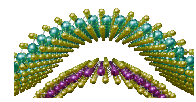
Figure 1: The peak of a WSe2/MoSe2 heterobilayer wrinkle. Wrinkles form on the 2D material surface due to various condition in synthesis or are applied on the 2D surface to produce desired properties. For example, they can lead to localized energy states at the peaks.
References
- Gjerding, M. N.; Taghizadeh, A.; Rasmussen, A.; Ali, S.; Bertoldo, F.; Deilmann, T.; Knøsgaard, N. R.; Kruse, M.; Larsen, A. H.; Manti, S.; others Recent progress of the computational 2D materials database (C2DB). 2D Materials 2021, 8, 044002.
- Liu, P.; Kaltak, M.; Klimeˇs, J.; Kresse, G. Cubic scaling GW: Towards fast quasiparticle calculations. Physical Review B 2016, 94, 165109.
- Schambeck, M.; Golze, D.; Wilhelm, J. Solving multipole challenges in the GW 100 benchmark enables precise low-scaling GW calculations. Physical Review B 2024, 110,125146.
- Bihlmayer, G.; Koroteev, Y. M.; Echenique, P. M.; Chulkov, E. V.; Bl¨ugel, S. The Rashbaeffect at metallic surfaces. surface science 2006, 600, 3888–3891.
- Varykhalov, A.; Marchenko, D.; Scholz, M.; Rienks, E.; Kim, T.; Bihlmayer, G.; S´anchez- Barriga, J.; Rader, O. Ir (111) surface state with giant Rashba splitting persists under graphene in air. Physical Review Letters 2012, 108, 066804.
- Daqiqshirazi, M.; Brumme, T. Funneling and spin-orbit coupling in transition metal dichalcogenide nanotubes and wrinkles. Physical Review B 2023, 108, 155304.
- Daqiqshirazi, M.; Brumme, T. Emergence of non-uniform strain induced exciton species in homo-and heterobilayer transition metal dichalcogenides. arXiv preprint arXiv:2406.08040 2024,
- Tyurnina, A. V.; Bandurin, D. A.; Khestanova, E.; Kravets, V. G.; Koperski, M.; Guinea, F.; Grigorenko, A. N.; Geim, A. K.; Grigorieva, I. V. Strained bubbles in van der Waals heterostructures as local emitters of photoluminescence with adjustable wavelength. ACS photonics 2019, 6, 516–524.
- Subakti, S.; Daqiqshirazi, M.; Wolf, D.; Linck, M.; Kern, F. L.; Jain, M.; Kretschmer, S.; Krasheninnikov, A. V.; Brumme, T.; Lubk, A. Electron holographic mapping of structural reconstruction at mono-and bilayer steps of h-BN. Physical Review Research 2023, 5, 033137.