
MATERIALS SCIENCE AND CHEMISTRY
From Molecules to Thin Films - GaP Nucleation on Si Substrates
Principal Investigator:
Ralf Tonner
Affiliation:
Theoretical Surface Chemistry Group, Philipps-Universität Marburg
Local Project ID:
GaPSi
HPC Platform used:
Hermit of HLRS
Date published:
Silicon is the most popular semiconductor material in science and industry. It is used for electronic devices with a variety of large-scale applications such as photo-voltaics and computer chips. Up to now, silicon is mainly used in microelectronic applications using its ability for electric conduction. Nevertheless, applications are reaching several physical limits mainly connected with the rapidly decreasing size of electric devices (e.g. transistors). To circumvent the technological bottleneck we are approaching, many ideas were put forward. One idea is to use light instead of electrons for signal transmission combined with the highly developed silicon manufacturing processes.
Silicon alone is thus not ideally suited to build theses optically active devices due to its fundamental physical property of being an indirect band-gap material. This means, it cannot be used as a laser material which is one of the major tasks of the research branch "Silicon Photonics" aiming at realizing these devices.
Building these devices relies on the knowledge about atomic and electronic structure of materials. Recently, two DFG-funded research programs (GRK 1782, SFB 1083) have been initiated with the aim to improve fundamental understanding and application of surface and interface processes. 21 research groups from several disciplines are involved in these programs at the Philipps-Universitaet Marburg.
The aim to combine silicon's electric properties with optically active parts can be achieved by growing layers of composit materials from group III & V elements onto silicon wafers. Laser-active quaternary compounds (GaNAsP) have thus to be grown with an intermediate layer of Galliumphosphide (GaP) to decrease the tension in the material. This GaP film is grown in an epitaxy process (MOVPE) from molecular precursor compounds.
This project's challenge is the simulation of the microscopic growth processes by _rst principles quantum-chemical computations in order to understand its chemical and physical details. This knowledge is not only valuable for similar material's growth procedures, it can also be utilized to directly influence the quality of our on-site semiconductor research by delivering the key parameters for successful growth. Those parameters include the reactivity of the precursors, the chemical processes at the substrate or the properties of the final film. The figure illustrates the growth phases from gas-phase to completed GaP films
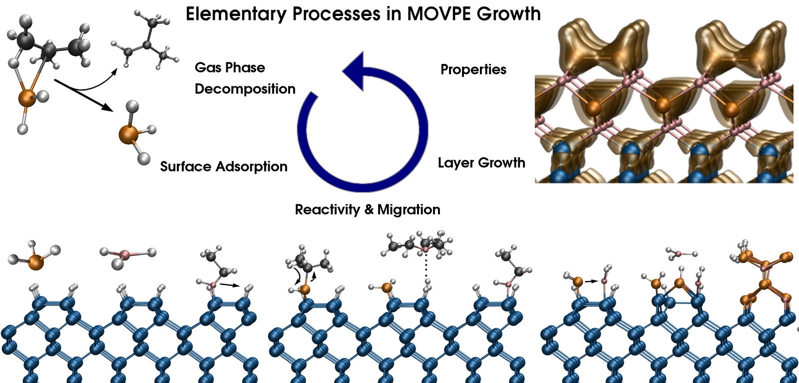
Fig. 1: Schematic representation of the MOVPE semiconductor growth on Silicon. © Philipps-Universität, Marburg
Furthermore, the chemical reactivity and bonding on surfaces is fundamentally different to the liquid or gaseous phase. The latter have been investigated for several centuries already whereas substrate-assisted processes became only accessible in recent decades due to advances in experimental and theoretical surface science (e.g. by Gerhard Ertl, Nobel Prize in Chemistry 2007). Those are extensively addressed here. Hence, a large community of researchers and industrial applications in the field of semiconductor materials as well as surface and catalyst science will benefit from this project's results.
The ab initio methodology (density functional theory) applied in this project delivers atomic and electronic properties of high accuracy for a large number of chemical events. This necessitates periodic models of the substrate and attached materials with up to 1,000 atoms and several thousand electrons which highly benefit from the GCS supercomputing capacities at the HLRS in Stuttgart.
Scientific Contact:
Dr. Ralf Tonner
Theoretical Surface Chemistry Group, FB Chemie
Philipps-Universität Marburg
Hans-Meerwein-Straße, D-35032 Marburg
e-mail: tonner@chemie.uni-marburg.de