MATERIALS SCIENCE AND CHEMISTRY

Materials Science and Chemistry

Principal Investigator: Ralf Tonner , Computational Materials Chemistry, Philipps-Universität Marburg

HPC Platform used: Hazel Hen of HLRS

Local Project ID: GaPSi

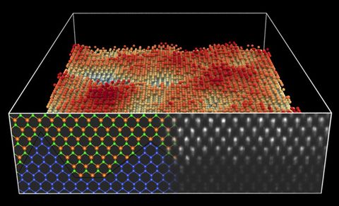
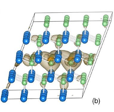
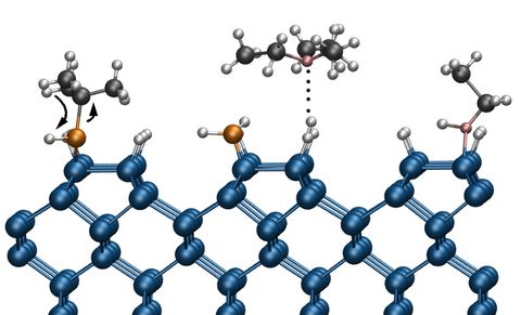
By applying approaches based on computational chemistry, researchers at the University of Marburg are addressing the challenge of designing functional materials in a novel way. Using computing resources at the High-Performance Computing Center Stuttgart, the scientists under leadership of Dr. Ralf Tonner model phenomena that happen at the atomic and subatomic scale to understand how factors such as molecular structure, electronic properties, chemical bonding, and interactions among atoms affect a material's behaviour.

Materials Science and Chemistry

Principal Investigator: PD Dr. Ralf Tonner , Philipps-Universität Marburg (Germany)

HPC Platform used: Hazel Hen of HLRS

Local Project ID: GaPSi

For the development of new communication and computing technologies, conceptually new materials and device architectures are needed. One pathway of increasing the efficiency of e.g. integrated transistor circuits is to implement photonic functionality to the devices. With the HLRS project “GaPSi”, researchers of the University of Marburg contribute to the developments in designing and producing optically active compound semiconductor materials that can be integrated into conventional silicon-based technology.

Materials Science and Chemistry

Principal Investigator: Ralf Tonner , Theoretical Surface Chemistry Group, Philipps-Universität Marburg

HPC Platform used: Hermit of HLRS

Local Project ID: GaPSi

Silicon is the most popular semiconductor material in science and industry. It is used for electronic devices with a variety of large-scale applications such as photo-voltaics and computer chips. Up to now, silicon is mainly used in microelectronic applications using its ability for electric conduction. Nevertheless, applications are reaching several physical limits mainly connected with the rapidly decreasing size of electric devices (e.g. transistors). To circumvent the technological bottleneck we are approaching, many ideas were put forward. One idea is to use light instead of electrons for signal transmission combined with the highly developed silicon manufacturing processes.