
MATERIALS SCIENCE AND CHEMISTRY
Realistic Modeling of Semiconductor Properties by First Principles Calculations
Principal Investigator:
PD Dr. Ralf Tonner
Affiliation:
Philipps-Universität Marburg (Germany)
Local Project ID:
GaPSi
HPC Platform used:
Hazel Hen of HLRS
Date published:
Ab initio calculations with large atomistic models are used to study chemical reactivity and physical properties related to nucleation, growth and interface formation critical for device functionalization of III/V semiconductors on silicon substrates. Precursor decomposition mechanisms determine the accessibility of novel metastable composite materials via chemical vapour deposition as well as dopant concentrations. In this project, the researchers analyzed several nucleation and decomposition trajectories with density functional theory. They also discovered that the interface morphology of the model system gallium phosphide on silicon is determined by both growth kinetics and the stability of local atomic configurations at the interface. Finally, the band structures of photonic materials were calculated with high accuracy and influences of chemical and strain effects were analyzed.
Motivation
For the development of new communication and computing technologies, conceptually new materials and device architectures are needed. One pathway of increasing the efficiency of e.g. integrated transistor circuits is to implement photonic functionality to the devices. With the HLRS project “GaPSi”, scientists of the University of Marburg contribute to the developments in designing and producing optically active compound semiconductor materials that can be integrated into conventional silicon-based (Si) technology.
Critical challenges are posed by the growth of nanoscale thin films of different III/V materials (i.e. elements from groups 13 and 15 of the periodic system) due to stability and kinetic effects. The researchers analyze the reactivity of precursor chemicals used during growth as well as the final materials' properties with accurate, parameter-free calculations of the atomic and electronic structure. Chemical reactivity and other elementary processes determine whether a certain material combination can be realized as intended for implementing new phenomena into computer chips or sensors communicating via light instead of electrons.
Computations
The scientists applied ab initio methods without experimental input parameters, namely density functional theory and wave function based quantum chemical methods in static and dynamic simulations, to describe the physical properties and reaction mechanisms relevant to semiconductor epitaxy via chemical vapor deposition. To achieve the necessary accuracy, firstly, a large number of reaction trajectories is often needed. The configurational space of an adsorbate close to a substrate can be highly complex and decomposition or surface diffusion dynamics depend strongly on a meaningful sampling of possible pathways.
Secondly, for calculating optical properties - e.g. band structures - of multinary compound semiconductor materials, large unit cells, and tight sampling of reciprocal space are needed. These requirements can only be met with large computational resources and the capability of running several trajectories in parallel. The HLRS provides optimal platforms to pursue this research and perform up-to-date calculations on a diverse range of questions in chemistry and materials science.
Results
In recent years, the reactivity of precursor molecules that carry III/V elements to the semiconductor substrate for functionalization has been in the focus of the PI's group. They examined decomposition mechanisms of gas phase and adsorbate species.[1-3] Efficient elimination of carbohydrate side groups is important to minimize defect contamination of the materials produced. Furthermore, crystal nucleation mechanisms are both of basic and applied research interest since they determine the material’s quality and the interface structure.

Fig. 01: Supercells of the Si(001) surface with different hydrogen coverages. Figure from [4].
Copyright: Computational Materials Chemistry, FB Chemie, Philipps-Universität MarburgOne aspect under investigation is computing the thermodynamic properties of the hydrogen passivation layer on Si substrates.[4] The coverage-dependent electronic and vibrational properties require large supercells as shown in figure 01.
The researchers applied different models (ab initio thermodynamics, interpolated and explicit phonon dispersion relations, Einstein model) for the evaluation of the equilibrium temperatures that allow activation of the H/Si(001) surface with respect to hydrogen desorption. Gallium phosphide (GaP) can be grown lattice-matched onto activated Si and represents a possible nucleation layer for further functionalization.
Another topic under investigation is studying chemical reactions related to GaP growth on H/Si(001) (precursor chemisorption in early nucleation)[5] and the resulting morphology and properties of the GaP-Si interface grown.[6] In close cooperation with chemical vapour deposition experiments, transmission electron microscopy analysis, and kinetic Monte Carlo modeling of growth processes, it was found that kinetic aspects enable the atomic structure to intermix within a region of eight atomic layers across the interface. On the other hand, thermodynamic stabilities determine pyramidal shapes to occur at the interface (figure 02) as was concluded from the scientists' first principles calculations applying large supercells.
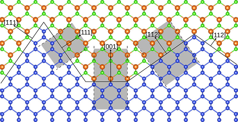
Fig. 02: Schematic of the GaP-Si interface morphology. The supercell models of different interface orientations used for the ab initio stability determination are indicated by shaded areas. Figure from [6].
Copyright: Computational Materials Chemistry, FB Chemie, Philipps-Universität MarburgFurthermore, strain and chemical influences on the band gaps of the optically active semiconductor alloys Ga(NAsP) and dilute Ga(AsBi) were investigated. Those can be used in device superstructures based on Si substrates with a GaP nucleation layer. Figure 03 shows the charge density of the valence band with two different local configurations of the Bi atoms in the GaAs lattice of dilute Ga(AsBi). The material's band gap largely depends on this local configuration which could be rationalized by solid state chemical bonding models.[7]
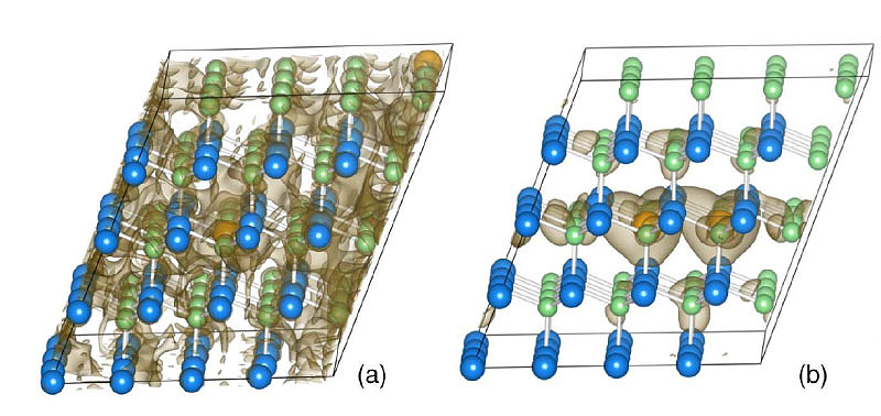
Fig. 03: Heavy hole valence band of Ga(AsBi) in a) a [111] chain and b) cluster arrangement of the dilute Bi atoms. Charge density integrated over the Brillouin zone at 10% of the maximum. Figure from [7].
Copyright: Computational Materials Chemistry, FB Chemie, Philipps-Universität MarburgAll of these studies were compared to experimental measurements on samples grown under commercially relevant conditions. Thus, the results were both directly related to larger-scale production of novel semiconductor materials as well as they have proven to be helpful in discovering new features, properties, or optimizing the growth conditions applied. Realistic models for ab initio calculations require large computational resources and reliable collaboration between theoretical and experimental scientists.
Acknowledgements
The researchers gratefully acknowledge the HLRS for providing computing facilities and IT support, the DFG via the research training group (RTG) 1782 and the Beilstein Institute for financial support.
References
[1-3] A. Stegmüller, P. Rosenow, R. Tonner, Phys. Chem. Chem. Phys. 2014, 16, 17018. A. Stegmüller, R. Tonner, Inorg. Chem. 2015, 54, 6363. A. Stegmüller, R. Tonner, Chem. Vap. Deposition 2015, 21, 161.
[4] P. Rosenow, R. Tonner, J. Chem. Phys. 2016, 144, 204706.
[5] A. Stegmüller, K. Werner, M. Reutzel, A. Beyer, P. Rosenow, U. Höfer, W. Stolz, K. Volz, M. Dürr, R. Tonner, Chem. Eur. J. 2016, 22, 14920.
[6] A. Beyer, A. Stegmüller, J. O. Oelerich, K. Jandieri, K. Werner, G. Mette, W. Stolz, S. D. Baranovski, R. Tonner, K. Volz, Chem. Mater. 2016, 28, 3265.
[7] L. C. Bannow, O. Rubel, S. C. Badescu, P. Rosenow, J. Hader, J. V. Moloney, R. Tonner, S. W. Koch, Phys. Rev. B 2016, 93, 205202.
Research Team
Andreas Stegmüller and Ralf Tonner, Philipps-University Marburg, Faculty of Chemistry and Material Sciences Center
Scientific Contact
Dr. Ralf Tonner
Computational Materials Chemistry, FB Chemie
Philipps-Universität Marburg
Hans-Meerwein-Straße 4, D-35032 Marburg
e-mail: tonner [at] chemie.uni-marburg.de
http://www.uni-marburg.de/fb15/ag-tonner
December 2016